Products
High-Density Interconnect (HDI) PCB & Microvia Technology
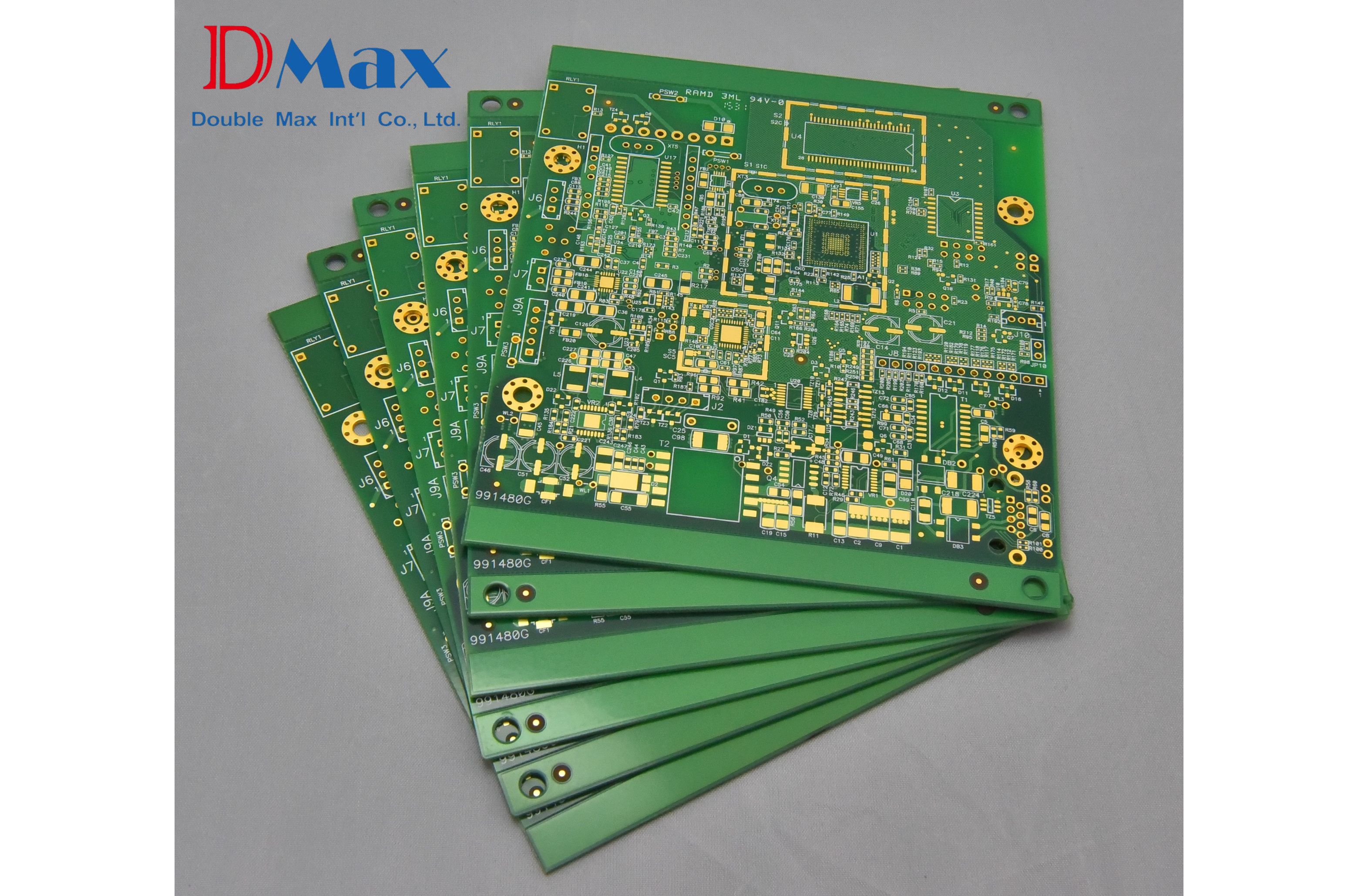
Service Overview : DMAX provides high-performance HDI PCB manufacturing with advanced laser drilling and microvia stacking for next-generation miniaturization.
-
Precision Engineering: Supporting 4-12+ layers with 3/3 mil fine-line processing and blind/buried vias.
-
Strategic Integration: 25+ years of expertise in horizontal and vertical supply chain coordination for components, fabrication, and testing.
-
High-Speed Performance: Optimized for 5G modules, AI vision systems, and compact medical diagnostics.
-

Online Quote
-

Upload PCB File
-

Order Review
-

Payment
-

Real-time Fabrication Tracking
-

Delivery
-

Confirm Received
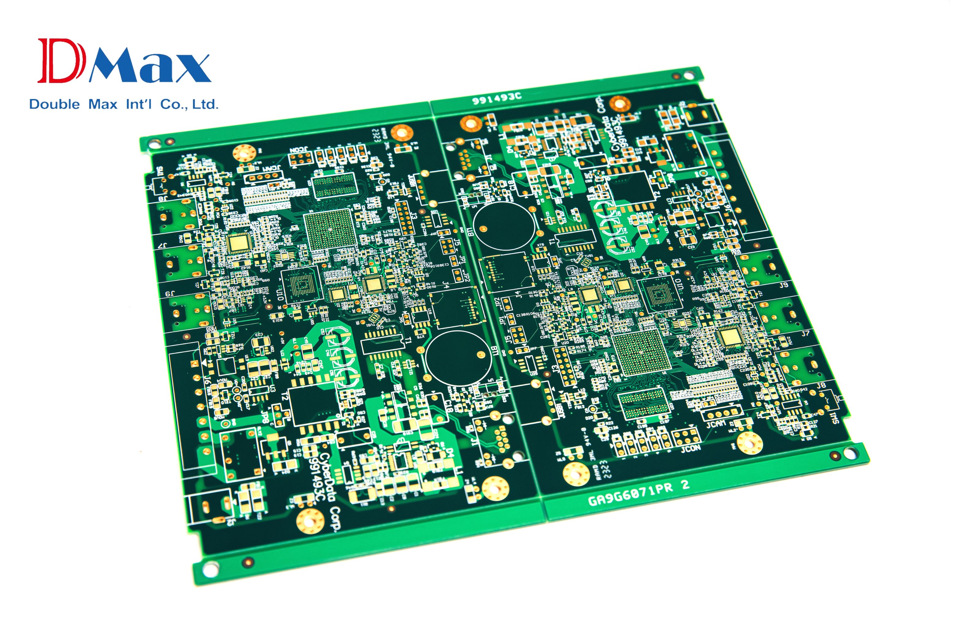
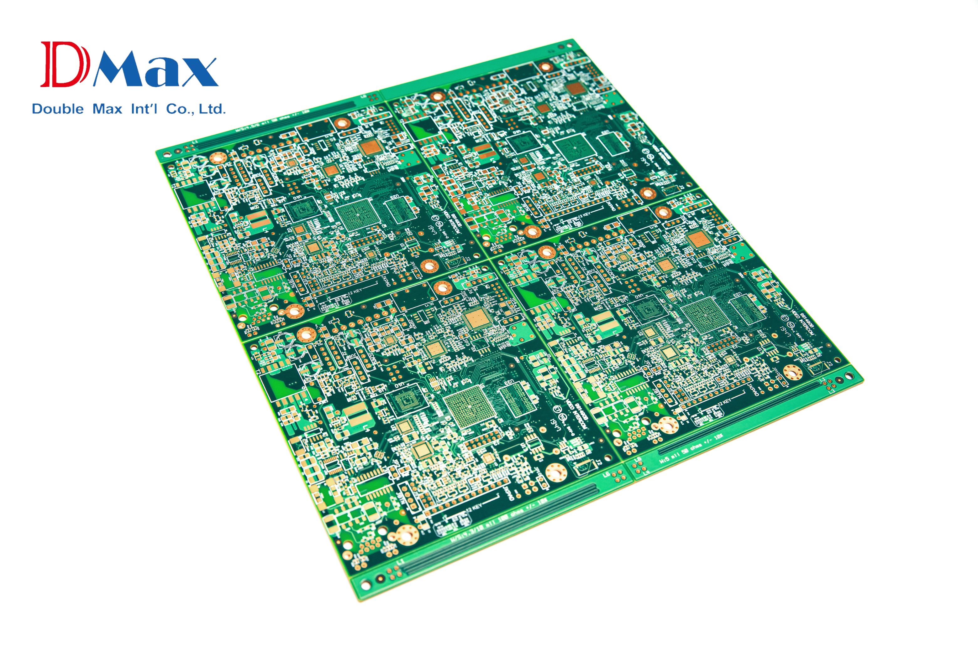
HDI PCB & Microvia Technology
Miniaturization Perfected. DMAX delivers high-performance HDI PCBs for compact, high-speed applications. With 25+ years of PCB expertise, we enable multilayer HDI fabrication that meets the most demanding signal integrity requirements.
Technical Capabilities & Customization
Microvia & Layer Stack-ups
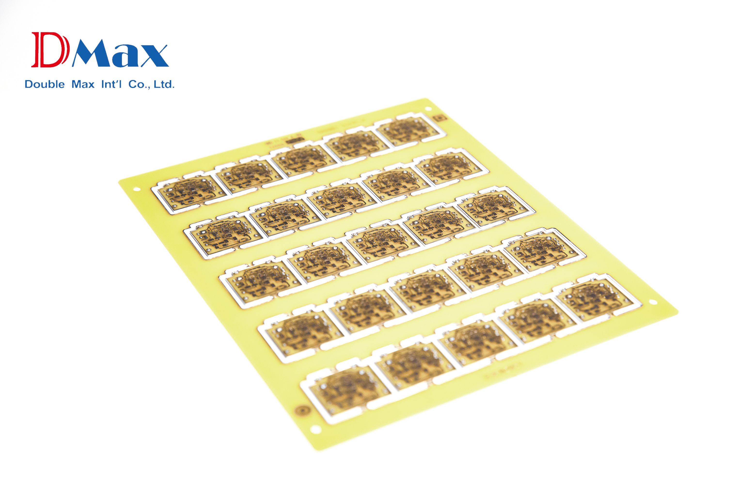
- Layers: 4 to 12+ layers with complex HDI structures.
- Via Technology: Laser-drilled microvias, stacked vias, and via-in-pad.
- Precision: Minimum line/space down to 3/3 mil or better.
Materials & Finishes
- Materials: High-Tg and low-loss dielectric for 5G/RF applications.
- Finishes: ENIG, ENEPIG, and OSP for superior SMT connectivity.
- Integrity: Impedance-controlled multilayer stack-ups (±10%).
Horizontal & Vertical Supply Chain Excellence
DMAX leverages a robust ecosystem of partners to provide a seamless, high-precision manufacturing journey from initial design to final deployment.
Vertical Integration
Coordinated procurement of industrial-grade components and specialized HDI substrates.
Horizontal Cooperation
Expert synergy with specialized PCB fabricators, inspection labs, and back-end assembly services.
Integrated Validation
Combined AOI, X-ray, cross-section analysis, and E-test per IPC Class 2/3 standards.
Typical Applications & Specialized Equipment
Telecom & 5G
5G base station modules, high-frequency communication boards, and networking gear.
AI & Smart Devices
AI vision processing boards, smartphones, tablets, and high-performance server SSDs.
Medical & Wearables
Implantable electronics, medical diagnostics, and advanced smartwatches/IoT modules.
DMAX is a premier Taiwan-based HDI PCB manufacturer with over 25 years of technical expertise in delivering high-density interconnect solutions. Our strength lies in our ability to collaborate horizontally and vertically across the supply chain, integrating laser-drilled microvias with precision SMT assembly for global leaders in 5G, AI, and medical electronics. Whether you need rapid NPI prototyping or scalable volume production, DMAX ensures consistent quality and signal integrity through IPC Class 3 compliant fabrication and advanced inspection services.
Innovate with High-Density Precision
Partner with DMAX for advanced HDI manufacturing and expert supply chain integration.
Inquiry Now +