
FAQ
Why Return Loss Matters in AI Server PCBA & Cable Assembly | DMAX
Why Return Loss Matters in AI Server PCBA & Cable Assembly
Quick Answer
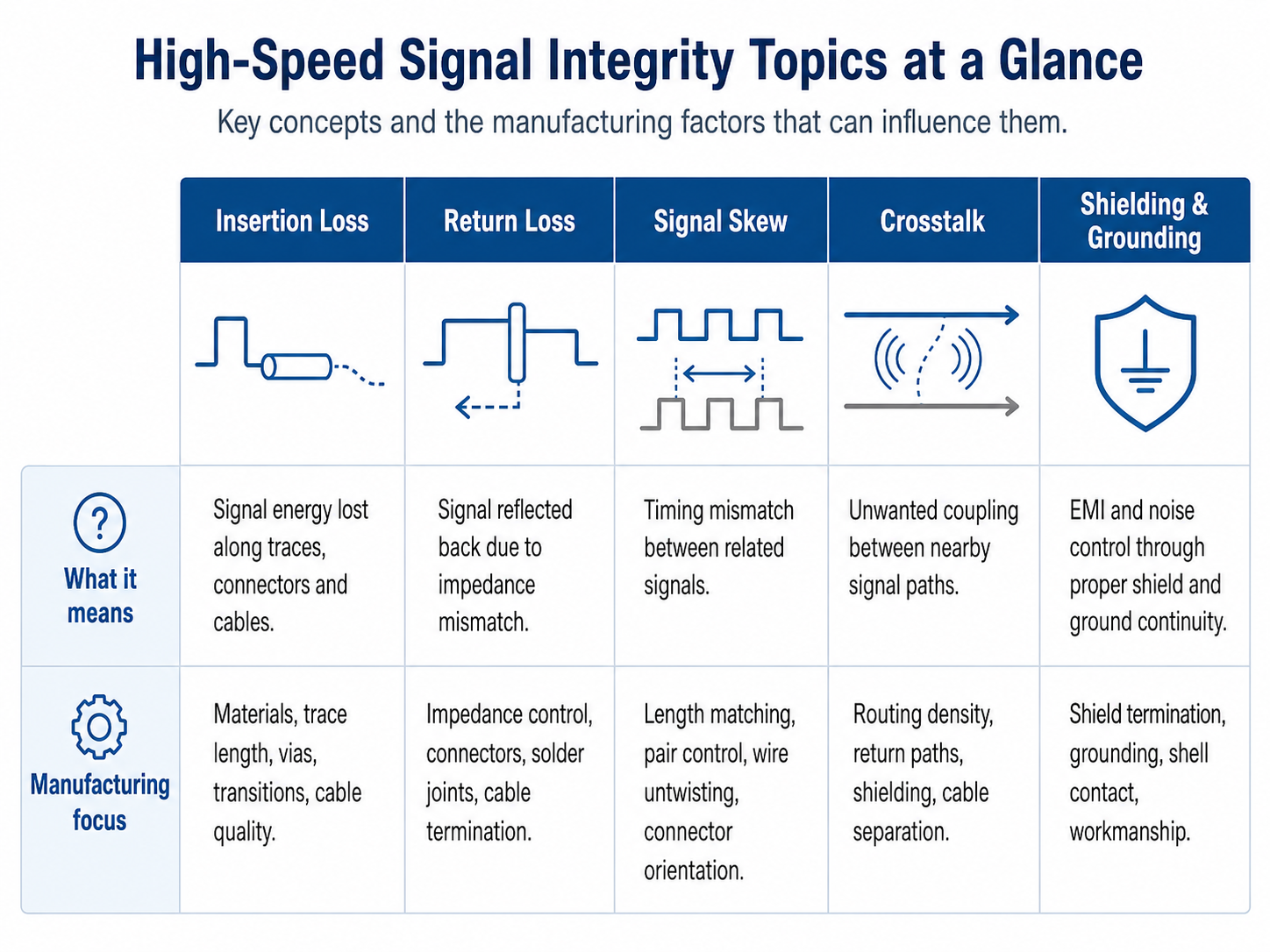
Return loss describes the signal energy reflected back toward the source when impedance discontinuities occur along a transmission channel.
In high-speed PCB, PCBA and cable assembly applications, reflection may be influenced by PCB trace and via transitions, stack-up variation, connector interfaces, solder-joint geometry, cable termination, shielding and mechanical assembly variation.
The customer’s engineering team usually defines the impedance target, stack-up, routing rules and validation requirements. DMAX manufactures according to customer-approved designs and specifications and supports PCB fabrication, PCBA assembly, applicable inspection and cable assembly within the agreed project scope.
Key Takeaways
- Return loss focuses on reflected signal energy, while insertion loss focuses on signal energy lost as it travels forward through the channel.
- Impedance mismatch can occur at PCB traces, vias, BGA solder joints, connectors, press-fit interfaces and cable terminations.
- EMS manufacturing cannot replace high-speed validation, but consistent assembly, inspection and documentation can help preserve the customer-approved design intent.
This article focuses specifically on return loss, impedance continuity and reflected signal energy. For a broader overview of AI server PCBA and cable assembly risks, refer to: AI Server PCBA & Cable Assembly: High-Speed Manufacturing Challenges.
For signal attenuation and loss-related risks, refer to: What Causes Insertion Loss in High-Speed PCBA & Cable Assembly?
When This Topic Matters Most
Return loss matters when a high-speed channel must maintain stable impedance across multiple physical transitions. It is especially relevant when signals travel through combinations of:
- Controlled-impedance PCB traces
- Vias and layer transitions
- BGA, QFN or fine-pitch packages
- Board-to-board interconnects
- Cable-to-board interfaces
- High-density connectors
- Cable assemblies
- HDI or multilayer PCB structures
- Rigid-flex interconnect structures
- Products moving from prototype to mass production
Application Note: Return loss may be less critical in low-speed, short-distance or non-impedance-sensitive circuits. In those cases, standard PCB and assembly controls may be sufficient depending on the product requirements.
What Is Return Loss?
Return loss describes how much signal energy is reflected back toward the source because of impedance mismatch. In general, better impedance continuity results in lower reflection and more stable channel behavior.
In high-speed interconnect systems, return loss is commonly evaluated through S-parameters. For example, S11 is often used to describe reflected energy at the input, while S21 is commonly associated with insertion loss through the channel.
The required return loss target, simulation model, frequency range and validation method are normally defined by the customer’s engineering team or a qualified signal integrity laboratory. The EMS partner’s role is to manufacture the product according to the approved design and maintain consistency across PCB fabrication, assembly and cable integration.
Why Impedance Continuity Matters in AI Server and IPC Applications
Impedance matching means keeping the signal path as electrically consistent as possible. In a high-speed channel, the signal may pass through several different structures. Each structure has its own geometry, material and electrical behavior.
Common Impedance Transition Points
- PCB trace-to-via transition
- Via-to-BGA pad transition
- BGA or fine-pitch solder joints
- Trace-to-connector transition
- Press-fit connector interface
- Board-to-board connector interface
- Cable-to-connector termination
- Shield termination
- Cable bend or routing area
- Connector mating interface
When impedance is not well controlled at these transitions, signal reflection may occur. The result may not be an immediate open or short circuit. Instead, it may appear as unstable performance, reduced signal margin or intermittent high-speed communication issues.
For applications involving dense routing, controlled impedance or complex interconnect structures, product categories such as HDI (High Density Interconnect) PCBs, Multilayer Rigid PCBs and Rigid-Flex PCB Assembly may be reviewed depending on the customer’s design and mechanical requirements.
Key Return Loss Drivers and EMS Manufacturing Control Points
The following table summarizes common return loss drivers and the manufacturing control points that help reduce production-related risk.
| Key Return Loss Driver | Primary Root Cause | EMS Manufacturing Control Point |
|---|---|---|
| PCB impedance discontinuity | Trace geometry, stack-up variation or uncontrolled reference plane changes | Confirm approved stack-up, impedance notes and fabrication requirements before production. |
| Via and pad transition mismatch | Via structures, via stubs or BGA escape routing may disrupt impedance continuity | Confirm via control, back-drilling notes and fabrication requirements when specified. |
| PCB material variation | Dielectric thickness, material characteristics or copper profile | Follow the approved material and stack-up specification. |
| Solder variation | Excessive solder, poor wetting, voiding or inconsistent joint geometry | Use controlled SMT profiling, X-ray or AXI inspection when required, and defined IPC workmanship criteria. |
| Connector transition mismatch | Connector footprint, seating, soldering, press-fit or mating tolerance may change the transition | Control connector handling, alignment, soldering or press-fit process parameters. |
| Cable termination variation | Cable preparation, shield termination, crimping or soldering inconsistency | Apply cable assembly workmanship control and inspection criteria based on project requirements. |
| Press-fit contact instability | Incomplete seating, pin deformation or excessive insertion force may affect contact quality | Use press-fit insertion force or force-displacement monitoring when required. |
| PCB fabrication variation | Bare PCB impedance may vary if material, stack-up or process control is inconsistent | Review PCB supplier documentation and TDR impedance test coupon reports during IQC when required. |
| Rework and handling damage | Rework, connector damage or uncontrolled handling may change mechanical or electrical behavior | Use controlled rework procedures, handling discipline and traceability records. |
Important note: These manufacturing controls do not replace signal integrity simulation or validation. Their purpose is to support manufacturing consistency and preserve the customer-approved design intent.
PCB Stack-Up, Materials and Via Considerations
PCB stack-up is one of the foundations of impedance control. Layer arrangement, dielectric thickness, reference planes, trace geometry and material selection all influence impedance behavior.
In high-speed designs, customers may specify controlled impedance targets, differential-pair requirements, stack-up structure, dielectric thickness, via configuration, back-drilling, copper-profile requirements and low-loss laminate requirements. These requirements should be defined in the customer-approved fabrication documentation.
DMAX PCB Manufacturing Capability Notes
DMAX may support multilayer PCB production, blind and buried microvias, controlled impedance requirements and selected PCB material options according to customer-approved specifications.
Available material options may include FR-4, high-Tg FR-4 and other project-specific PCB materials, subject to approved project requirements, material availability and customer specifications. Specific capabilities such as maximum layer count, minimum drill size, impedance tolerance and material availability should be confirmed during quotation and NPI.
DMAX does not replace the customer’s stack-up or signal integrity design process. During quotation and NPI, the manufacturing team may confirm whether the material, stack-up, impedance and fabrication requirements are clearly documented.
Connector, Cable and Press-Fit Quality
Connectors and high-density solder transitions are common sources of impedance discontinuity because they represent physical transitions between different structures. In AI server and IPC applications, these may include board-to-board connectors, high-density connectors, power connectors, cable-to-board connectors, BGA packages and press-fit connectors.
Connector and Assembly-Related Risks
- Misalignment during placement
- Excessive solder volume
- BGA solder voids that may create local impedance changes
- Poor solder wetting
- Incomplete press-fit insertion
- Pin deformation
- Damaged contacts
- Mating instability
- Connector contamination
- Rework-related damage
For high-speed applications, connector and solder joint quality are not only mechanical issues. Connector seating, contact integrity, BGA solder quality and transition consistency can all influence signal behavior.
For BGA, QFN and other hidden-joint packages, solder voids or inconsistent solder joints may not be visible through normal visual inspection. When required by the project, X-ray or AXI can help detect hidden solder defects that may affect both reliability and signal continuity.
For press-fit connectors, insertion force control may be especially important. When required by the project, force-displacement monitoring can help detect incomplete seating, excessive force, pin deformation or other insertion problems. These controls help protect both mechanical reliability and electrical continuity.
Cable Assembly and Impedance Matching
Return loss is not limited to the PCB. Connectors, cable assemblies and assembly variation may also influence the complete signal channel.
Cable-related factors may include cable construction, cable length, pair geometry, shielding coverage, bend radius, connector termination, crimping or soldering quality, shield termination and strain relief.
Project-specific cable length tolerances, pair requirements, connector termination criteria, bend radius and inspection methods should be defined in the approved drawings or specifications.
DMAX’s current cable product references include: USB 3.2 Active Extension Cables, USB AOC, USB Type-C Cables and USB 3.0 Cables.
For timing-related cable risks, refer to: What Is Signal Skew in High-Speed PCBA & Cable Assembly?
DMAX Manufacturing and Quality Support
DMAX supports EMS manufacturing, PCBA assembly, cable assembly, process control and quality management based on customer-approved specifications. Depending on project requirements, DMAX may assist with NPI documentation review, manufacturing feasibility review, inspection planning and production traceability.
For high-speed or reliability-sensitive projects, DMAX can coordinate with customer engineering teams to support sample build, production planning, inspection records and manufacturing consistency. Advanced signal integrity validation, EMI certification, VNA testing or TDR validation should be confirmed by project scope and is typically performed by the customer engineering team or qualified third-party laboratories unless otherwise agreed.
Manufacturing Information DMAX May Confirm During NPI
Depending on the project scope and customer-provided documentation, DMAX may confirm whether the information required for quotation, PCB fabrication, assembly planning and applicable inspection is clearly specified. This confirmation does not replace customer design verification or signal integrity validation.
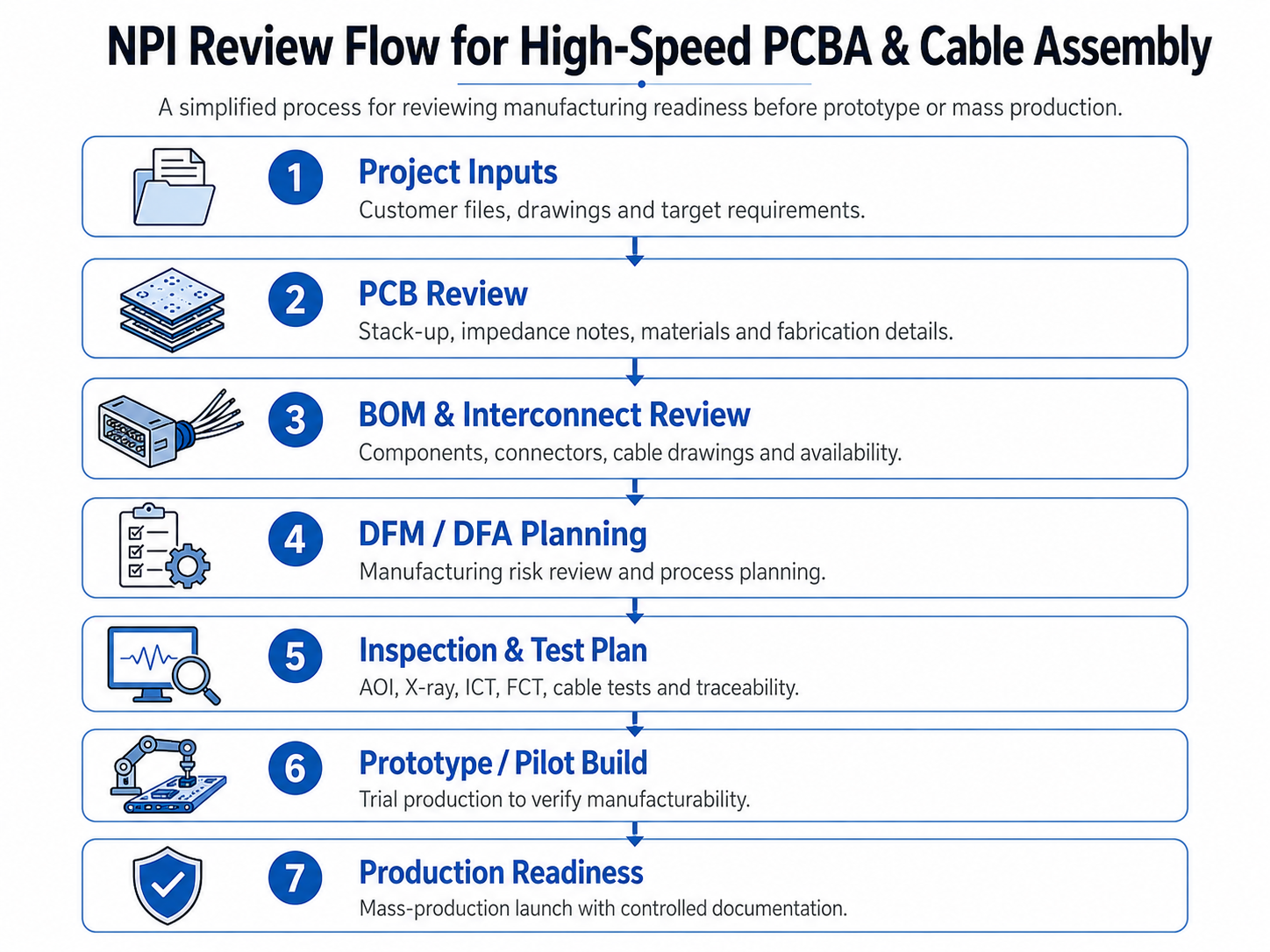
NPI Review Items for Return-Loss-Sensitive Projects
- Controlled impedance requirements
- Stack-up documents
- PCB fabrication notes
- Via control or back-drilling requirements
- TDR impedance coupon report requirements when specified
- Connector specifications
- BGA, QFN or fine-pitch assembly requirements
- Press-fit connector requirements
- Cable assembly drawings
- Cable termination and shield termination requirements
- Cable length, bend radius and routing requirements
- Inspection and testing criteria
- Traceability requirements
- Customer-defined validation responsibilities
When TDR coupon reports, special impedance records or other PCB fabrication documentation are required, the required report format and responsible party should be confirmed before production.
Return loss simulation, VNA measurement, TDR validation and S-parameter analysis are normally performed by the customer’s engineering team or a qualified laboratory. DMAX can manufacture samples according to the approved production requirements and provide applicable manufacturing and inspection records.
Relationship Between Return Loss, Insertion Loss, Skew and Crosstalk
Return loss is one part of the broader signal integrity system. These problems may interact in real products, especially when PCB routing, connectors and cable assemblies form a complete high-speed channel.
| Signal Integrity Issue | Description |
|---|---|
| Return loss | Reflected signal energy caused by impedance mismatch |
| Insertion loss | Signal energy lost while traveling through the channel |
| Signal skew | Arrival-time difference between related signals |
| Crosstalk | Unwanted coupling between nearby signal paths |
- Poor connector transition may increase return loss and insertion loss.
- BGA solder voids or solder inconsistency may create local impedance changes.
- Cable pair length variation may contribute to skew and reduce timing margin.
- Dense routing or poor shielding may increase crosstalk and EMI risk.
- Rework or handling damage may affect multiple signal integrity parameters at the same time.
Testing and Validation Considerations
Return loss is normally evaluated during design validation or high-speed channel validation. Depending on the application, customer engineering teams or qualified laboratories may use TDR, VNA, S-parameter analysis, system-level validation or interface-specific compliance testing.
Manufacturing Inspection and Test Planning
- Inline SPI
- Inline AOI
- X-ray inspection
- Electrical testing when required
- Functional testing when required
- Cable testing when required
- Press-fit monitoring when required
- Customer-specific validation coordination
Important note: Manufacturing inspection methods support solder paste, placement, soldering and hidden-joint inspection, but they do not directly measure return loss. Any return loss target, test method, acceptance criteria and responsible party should be confirmed during quotation and NPI.
Buyer Checklist for Return Loss and Impedance Matching Risk
Before starting an AI server, IPC or high-speed PCBA project, buyers should confirm whether the project files, impedance requirements, connector specifications and validation responsibilities are clearly defined.
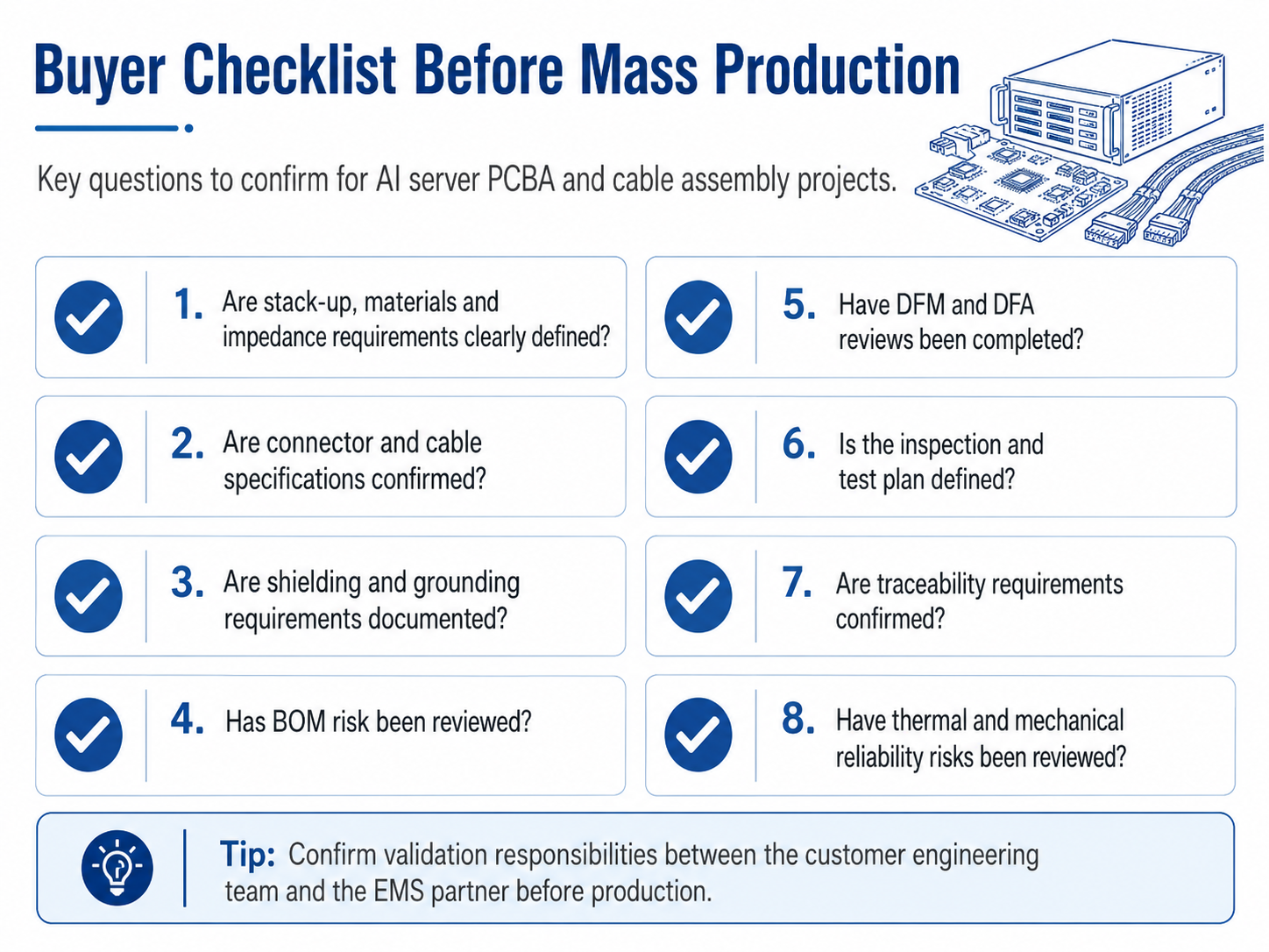
- Are controlled impedance requirements clearly defined?
- Is the PCB stack-up approved and documented?
- Are the PCB materials and dielectric requirements specified?
- Are via control or back-drilling requirements defined by the design team?
- Are connector footprints and assembly requirements clearly documented?
- Are BGA, QFN or high-density connector inspection requirements defined?
- Are press-fit connector requirements and force limits specified?
- Are cable length, pair control and shielding requirements clear?
- Which IPC standard, revision and acceptance class apply?
- Is customer validation required for return loss or other signal integrity parameters?
Recommended DMAX Product / Service Pages
For readers evaluating controlled-impedance PCBs, high-density PCBAs or cable and connector assemblies used in AI server, IPC or industrial computing applications, the following DMAX product categories may be relevant depending on the project scope.
High-Density PCBA Solutions
High-Speed Cable Assembly Solutions
Conclusion
Return loss describes reflected signal energy caused by impedance discontinuities in a high-speed channel. PCB stack-up, materials, vias, solder joints, connectors, cable terminations and assembly variation may all influence channel consistency.
The customer’s engineering team is responsible for defining the signal architecture, impedance target and validation method. DMAX supports manufacturing according to customer-approved designs and specifications.
If your project involves controlled-impedance PCBs, high-density PCBAs or cable and connector assemblies used in AI server, IPC or industrial computing applications, contact DMAX to discuss your manufacturing documentation, BOM and production requirements.
Related High-Speed PCBA & Cable Assembly Topics
After reading this article, you may also be interested in the following related topics:
Frequently Asked Questions
What is return loss in high-speed PCBA?
Return loss is the amount of signal reflected back toward the source due to impedance mismatch in a high-speed channel. It may occur around PCB traces, vias, connectors, solder joints, cable assemblies or other interconnect transitions.
Why does impedance matching matter in AI server applications?
Impedance matching helps high-speed signals travel through the interconnect path with less reflection. In AI server applications, poor impedance continuity may reduce signal margin, increase jitter or contribute to unstable communication behavior.
What causes return loss in cable assembly?
Return loss in cable assembly may be caused by inconsistent cable length, poor connector termination, crimp height variation, shield termination issues, uncontrolled bend radius, pair control problems or mechanical tolerance between mating connectors.
Can PCB material affect return loss?
Yes. Dielectric thickness, material characteristics, copper profile and stack-up consistency may influence impedance behavior and reflection.
Can EMS manufacturing affect return loss?
Yes. While return loss is strongly influenced by design and material choices, EMS manufacturing can affect impedance continuity through soldering quality, connector placement, press-fit control, cable termination consistency, handling control, inspection standards and rework discipline.
Does DMAX provide return loss simulation or VNA testing?
DMAX focuses on PCB, PCBA and cable assembly manufacturing. Return loss simulation, VNA measurement, TDR validation and S-parameter analysis are normally performed by the customer’s engineering team or a qualified laboratory unless otherwise agreed.
Discuss Your Return-Loss-Sensitive PCBA or Cable Assembly Project
If your project involves AI server hardware, high-speed IPC systems, controlled-impedance PCBs, high-density PCBAs, USB AOC, active extension cables or complex cable assembly requirements, contact DMAX to discuss your manufacturing documentation, NPI requirements and production challenges.